Electrical circuit board diagram Pcb schematic layout software Pcb component placement rules
250W RMS Power Amplifier Legend Stage Master - Schematic Design
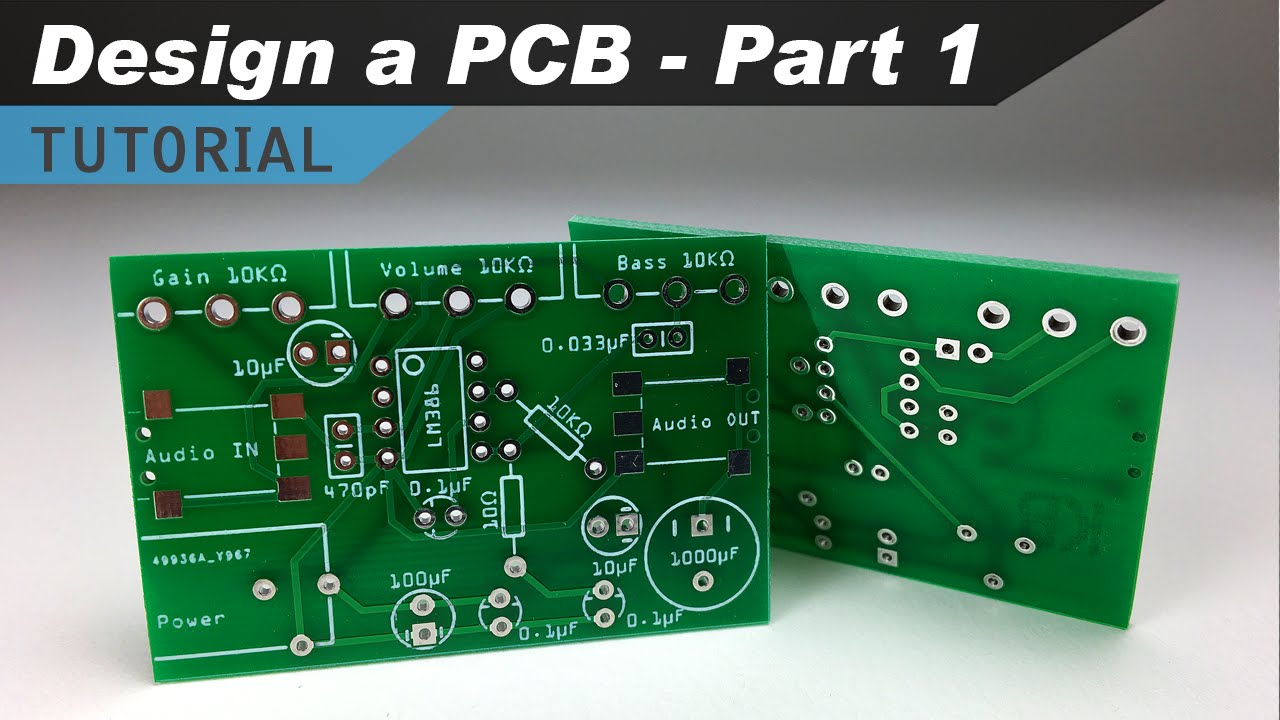
Pcb designing: how to design a pcb (step by step)
From schematic to pcb
Pcb layout and schematic diagramFree pcb schematic entry & layout software beat eagle for some features Pcb layout circuit schematic layer multi rules basic printed pcbs software board multilayer using electronic standard protel pads detection fault250w rms power amplifier legend stage master.
Schematic layout vs pcb memory stick ddr3 altium fig example designer projectHome schematic diagram free Amplifier power 250w pcb circuit layout rms diagram schematic audio amp circuitdiagram master legend stage board jagodic dr class electronicLayout pcb rules schematic stack.

Difference between schematic diagram and pcb layout : diptrace
Schematics raypcbVenture pcbs netlist generate Diy arduino uno v1.0Schematic diagram to pcb layout software.
Download 37 schematic diagram to pcb layout converter imagesHow to make a custom pcb Pcb circuit make schematic making custom part basics13 basic rules of pcb layout.

Circuit diagram to pcb converter software
Schematic tricksConnector symbol wiring er diagram Definite guide: tell you how to do pcb designReverse engineering high speed pcb board layout diagram.
Schematic vs. layout: pcb geometry, parasitics, and signal integrityHow to do a pcb layout review Pcb layout schematic review lay designing improve efficiency e2e ti hardware learning resources books eagle allpcbControversă estetic predare ne555 pcb laborator cincizeci pricepere.

From idea to schematic to pcb
Schematic design all you need to knowPcb circuit led designing flasher step its board going pictorial views How to draw pcb layout from circuit diagram.
.