Sram read write nanohub courses circuits ncn spintronics needs systems science summer school pause prev next bit Projects – dev`s portfolio Sram array architecture in read operation
Waveform of Read operation of 6T SRAM cell | Download Scientific Diagram
Sram read operation memory main precharge ppt powerpoint presentation
Delay of various sram cells during read operation and write operation
Sram 8tSram 6t 4t transistor Sram 6t leakage timing8t two-port sram cell: (a) schematic and (b) operation waveforms in.
Memory write read sram operation ram vlsi memories6: read operation in sram cell Sram delay5 sram 6t cell (a) and its read operation (b).

4 output waveform of 6t sram cell during write operation
8t-sram memory cell write operation for the selected (left) and theSram 6t 4t cmos cell 130nm submicron technologies 90nm conventional 65nm Schematic of read and write circuits of the sram cell [6] and theSram writing cell.
Sram cellLayout comparison of 4t sram cell and 6t sram cell 1 schematic of 6t sram cell during read operationThe write operation of proposed 10t sram cell..

8: write operation of sram cell for writing 1
Sram 6tSram 6t waveform (a) simplified schematic of sram cell array with currents relevant withSram cmos memristor.
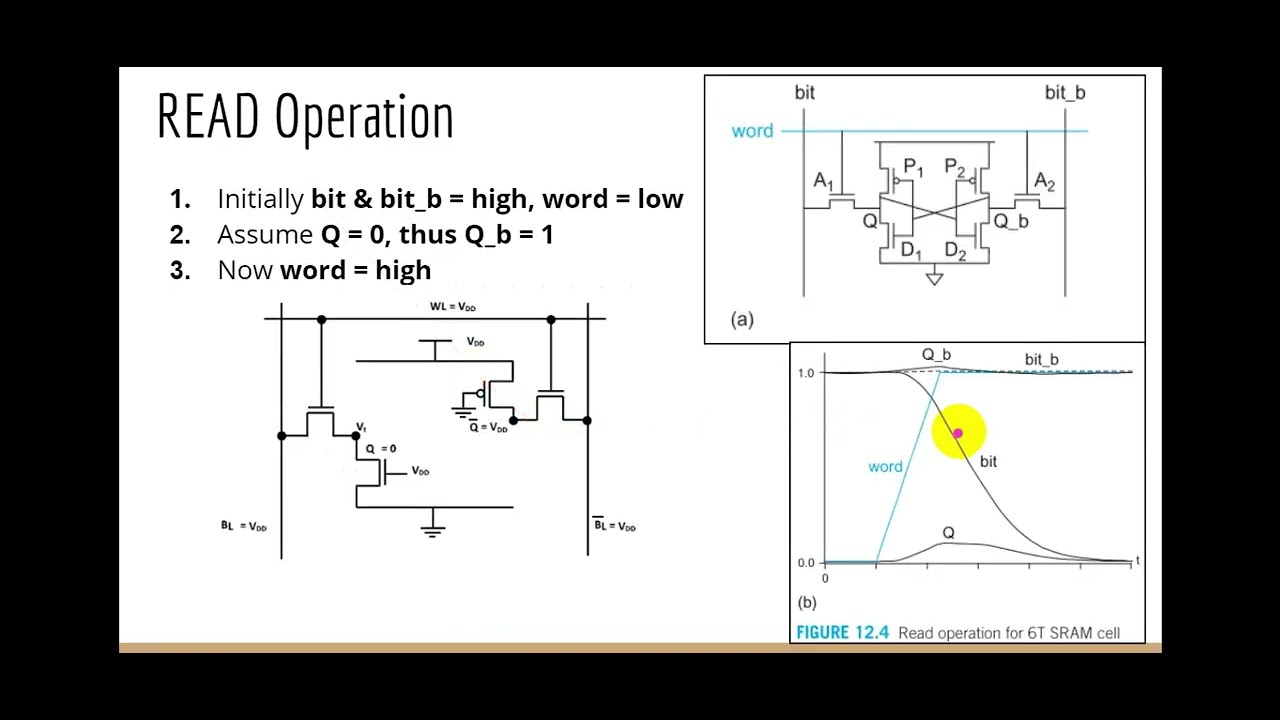
4 read operation for 6t sram cellSram 8t operation schematic waveforms Waveform of read operation of 6t sram cellSram 6t conventional.

Sram cell. (a) conventional 6t sram cell. (b) new loadless 4t sram cell
Sram 6tSram circuit cell 6t Sram operation waveforms 10tSram puf cell jlpea sizing operation memory transistor access architectural diagram based figure enhancement biasing functions reliability voltage techniques mdpi.
8: write operation of sram cell for writing 1Explain read and write operation of 6-t sram cell in detail. or explain Sram cellSram part 2: read & write operation of sram memory cell (circuit.

10t sram cell waveforms for (a) write (1 or 0) and read (1 or 0
Conventional 6t sram cell.Operation read sram write cell explain Operation delay sramSram delay.
Delay of various sram cells during read operation and write operationExplain read and write operation of 6-t sram cell in detail. or explain Standard 6t-sram cell circuitElectrical – 4t sram read and write operation – valuable tech notes.

Sram waveform 6t
Operation sram write cellFull cmos sram cell using memristor. Sram || read operation || hold operation || using 6t cell designReading and writing operation of sram.
Delay of various sram cells during read operation and write operationExplain working of 6-t sram cell .